The Innovation
The modular approach of the new concept of QDA technology associated to a digital implementation up to the PAs, permits higher flexibility on addressing a wider range of applications, with different types of signals and bandwidth needs, by a simple firmware upload. Also, the power amplifier hardware that can be implemented in diverse technologies (CMOS – Complementary Metal Oxide Semiconductor, GaN – Gallium Nitrite, GaS – Gallium Arsenide and Bipolar).
QDA uses in the signal processing a digital quantization to generate the quantization components with a constant envelope that are amplified separately by optimized switched amplifiers with different power outputs. We developed a new signal processing optimization called “digital pulse shaping of quantization noise” that allows a reduction of the number of amplification branches, improves the efficiency, and reduces both the in-band and out-of-band quantization noise to levels below -50dB.

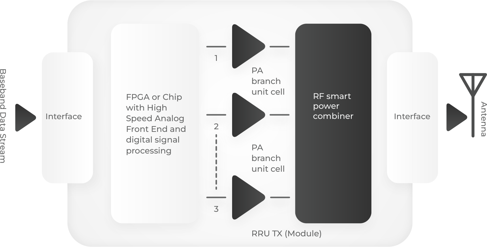
QDA can be composed of a high-performance FPGA, including RF bandwidth analog-to-digital converters (ADCs) and digital-to-analog converters (DACs), or by a chip that integrates both signal processing parts of FPGA, DACs, ADCs, and mixers for up-conversion. It is followed by a set of RF power amplifier branches, each one optimized for an adequate power level. The last block is a RF power combiner especially designed for QDA, which is digitally controlled by the FPGA or the chip for optimum energy efficiency operation.
Given the versatility of the technology, the QDA amplifier can be used at all points in the telecommunication system where there is an antenna.
